PCB Design Services
Pristine is a premier services provider in the design and development of Embedded Systems Software. We provide design and development services for Firmware, Device Drivers, Communication Protocols, and Embedded Software.
Pristine PCB layout engineers working with world-wide customers deliver "First time right designs”. The stringent process, continual training programs on current technologies are the keys for the success of the company.
The experience acquired from handling highly complex PCB designs for cutting-edge technologies spread across major Industry Verticals like Military, Aerospace, Telecom, Medical, Automotive, Industrial and consumer electronics.
“Quickest Turnaround Time”- With flexible working hours, multiple resources, shifts (24 X 7), skill programs and Stringent Quality Checks, ensure that extreme turnaround time challenges are achieved for customers.
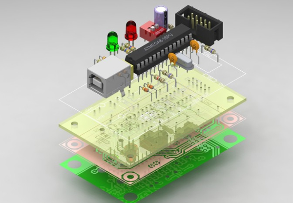
We developed & employ the proven PCB design process & Quality checks for the complete design flow from the start to the manufacturing release to ensure the design meets all the specifications & to increase the efficiency.
No matter what Printed circuit board (PCB) design program, the process is followed commonly for low to high complex PCB designs to ensure the best quality all times. We at Pristine, constantly develop, tune & use the custom programs to help achieve greater efficiencies & to improve quality by reducing the manual effort.
High speed Digital designs, Analog designs, mixed designs, power designs & RF design
Signal Integrity, EMC & EMI Compliant designs
PCBs with DFM, DFT, DFA requirements
PCBs for Pb-free, RoHS, EuP certifications
PCBs with Controlled impedance requirements
PCBs for mechanical constrained designs
PCBs for Flexi, Rigid & Rigid-Flex designs
PCBs for Mobile phone designs with ALIVH technology
HDI designs with via-in-pad, blind via, buried via & micro vias
Effectively used via stacking & staggering technology
High frequency PCBs of up to 10Gbps
High layer count PCBs of up to 38 layers
Dense PCBs with pin count of 10000+ pins
PCBs with high pin density of 540 pins/sq. inch
High component count PCBs; > 6000 components
Designs with fine pitch BGAs of 0.4mm & 0.5mm
Designs with high pin count full matrix BGA 1422pins with 0.5mm pitch
Designs with 3mils/3mils trace & spacing
Over 100+ complex and HDI designs completed in 15 years.
Expertise in High speed digital, Mixed signal, Analog & Power boards.
Innovative design methods in Fine Pitch Micro BGA designs.
Handled upto 0.37mm BGA pitch designs with 2 mil/ 2mil track/spacings.
Design technologies with stacked and staggered µ via HDI technology.
Integrating Mechanical & Electrical CAD data for assembly verification.
Board level, System level SI , PI, EMI/EMC & Thermal analysis.
High bit rate (~ 15Gbps) analysis for serial I/O designs.
Signal performance analysis for Reflections, Timing, BER, EYE opening.
DC drop analysis in power supply rails due to copper losses.